
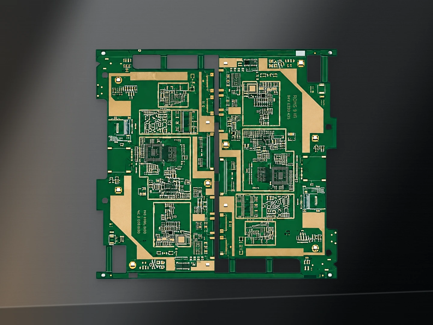
HDI PCB Manufacturing
Professional HDI PCB fabrication with micro-vias, blind/buried vias, fine-pitch BGA support and sequential lamination. High-density multi-layer boards from prototype to volume production.
- Product reference
- hdi-pcb-manufacturing
- Availability
- Confirm with our team
Description
HDI PCBs use advanced fabrication techniques to achieve higher wiring density than conventional multi-layer boards. By incorporating micro-vias (typically laser-drilled), blind vias, buried vias, and thinner dielectric layers, HDI designs allow more routing channels in a smaller area while maintaining excellent signal integrity and power distribution.
Key advantages of HDI technology include:
- Significant reduction in board size and layer count for the same functionality
- Improved electrical performance with shorter signal paths and lower inductance
- Reliable support for fine-pitch BGA, QFN, and CSP packages
- Better thermal management and higher component density
- Enhanced mechanical reliability through optimized via structures
We manufacture HDI boards using sequential lamination processes, precise laser drilling, and controlled plating to ensure consistent via quality and high yields. Surface finishes such as ENIG are commonly used to support fine-pitch assembly and wire bonding when required.
Our production supports both prototype and high-volume runs, with strict process control on registration, impedance, and surface quality. Panelized designs are optimized for efficient manufacturing and assembly.
Key HDI Capabilities
- HDI Structure: 1+N+1, 2+N+2, and higher sequential build-up
- Micro-vias: Laser-drilled, typically 0.075–0.15 mm diameter
- Via Types: Blind vias, buried vias, stacked or staggered micro-vias, via-in-pad
- Minimum Trace/Space: Down to 2.5/2.5 mil or finer (design dependent)
- Layer Count: Up to 20+ layers with HDI construction
- Materials: High-Tg FR-4, low-loss materials, and specialized laminates
- Surface Finish: ENIG (preferred), Immersion Silver, OSP, Soft/Hard Gold
- Special Features: Via-in-pad (filled & capped), fine-pitch BGA support, impedance control
- Testing: AOI, flying probe, impedance testing, cross-section analysis
Typical Applications
- Smartphones, tablets, and wearable devices
- High-density computing and AI accelerator modules
- Medical electronics and implantable devices
- Automotive ADAS, radar, and camera modules
- Communication and 5G/ RF modules
- Industrial high-density controllers
- Aerospace and defense electronics
- Consumer electronics requiring miniaturization
Why Choose Our HDI PCB Service
- Proven capability in complex HDI stack-ups and micro-via processes
- Strong support for fine-pitch BGA and high-density designs
- Consistent quality with advanced process control and inspection
- Flexible production from quick-turn prototypes to volume manufacturing
- Full engineering support including DFM review and stack-up optimization
- Seamless integration with PCB assembly (PCBA) services
Send us your design files, stack-up requirements, or Gerber data. We provide free DFM analysis and competitive quotation for HDI PCB prototypes and production orders.
We specialize in High Density Interconnect (HDI) PCB manufacturing for advanced electronic products that require higher component density, finer traces, and superior signal performance. HDI technology enables smaller board sizes, better electrical performance, and reliable connections for fine-pitch BGA, CSP, and high-pin-count devices.
Our HDI capability covers laser-drilled micro-vias, blind and buried vias, via-in-pad designs, and sequential build-up processes. The boards shown in production panels and complex layouts demonstrate our ability to deliver precise, high-reliability HDI PCBs for demanding applications.
Ready to discuss this product?
Share the application, quantity, current files and testing requirements. We will help define the next practical step.