
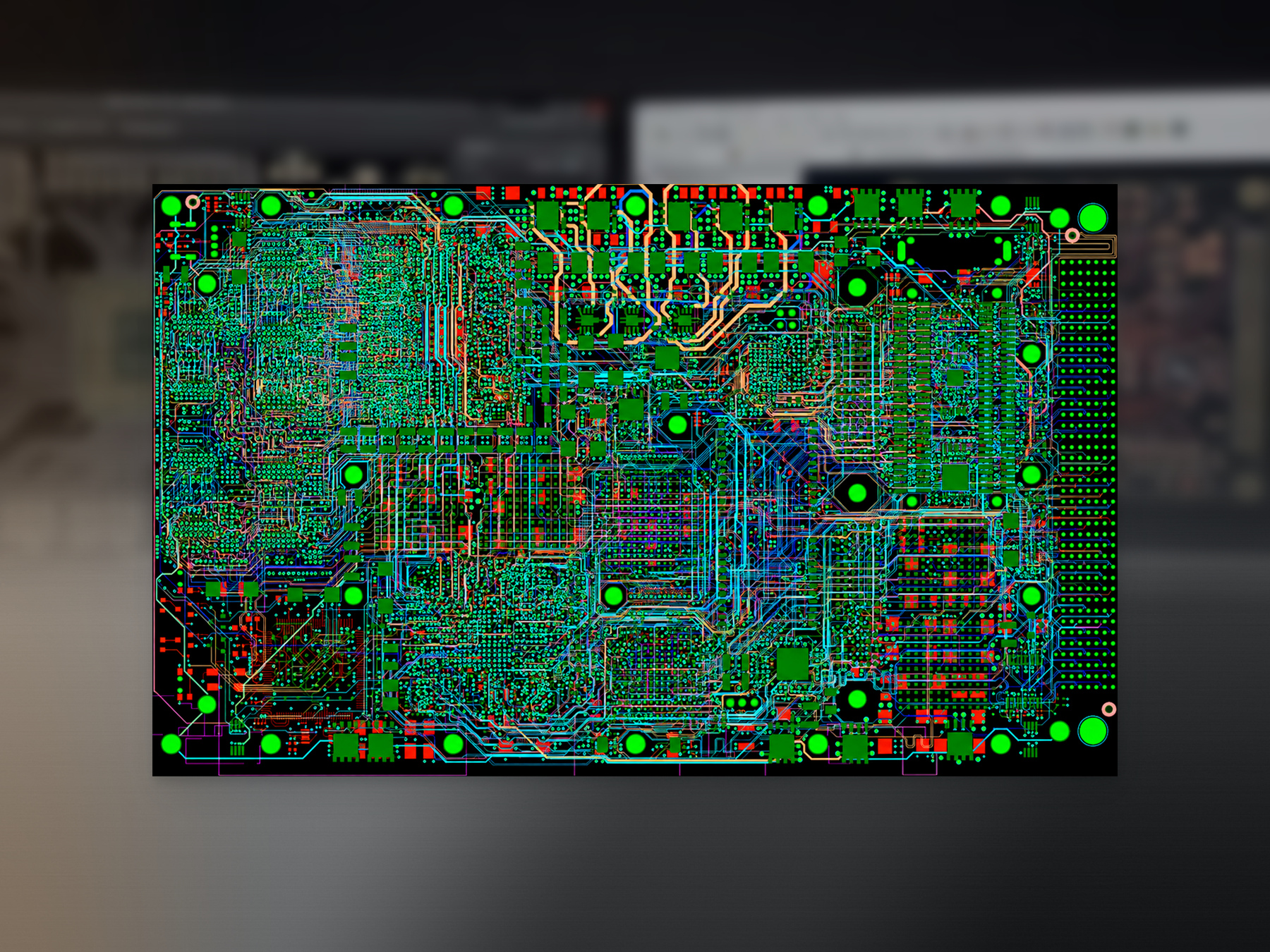
Professional PCB Design Service
Expert PCB design services including schematic capture, multi-layer layout, HDI, Rigid-Flex, high-speed & impedance control. From concept to production-ready Gerber files with full DFM support.
- Product reference
- professional-pcb-design-service
- Availability
- Confirm with our team
Description
Good PCB design is the critical bridge between your electronic concept and a successful product. Poor layout can cause signal integrity issues, EMI problems, thermal failures, or manufacturing difficulties. Our design team focuses on creating robust, production-ready boards that minimize risk and reduce time-to-market.
We support a full range of design requirements:
- Schematic capture and circuit optimization
- Component selection and library creation
- Multi-layer PCB layout (up to high layer counts)
- High-density interconnect (HDI) and micro-via designs
- High-speed digital, differential pairs, and controlled impedance routing
- RF / microwave and mixed-signal layouts
- Rigid-Flex and flexible circuit design
- Power integrity and thermal considerations
- Design for Manufacturing (DFM) and Design for Assembly (DFA)
Our process includes careful layer stack-up planning, proper return path design, length matching, crosstalk control, and comprehensive design rule checks. We deliver complete manufacturing packages including Gerber files, drill files, pick-and-place data, BOM, and assembly drawings.
Key Design Capabilities
- Schematic Design: Capture, simulation support, and circuit review
- Layout Complexity: 2–40+ layer boards, fine-pitch BGA, 01005 components
- High-Speed Design: DDR, PCIe, USB, Ethernet, SerDes, length matching & impedance control
- HDI Technology: Micro-vias, via-in-pad, sequential lamination support
- Special Designs: Rigid-Flex, high-current, high-voltage, RF, and mixed-signal
- Stack-up & Materials: Optimized for cost, performance, and manufacturability
- Analysis Support: Basic signal integrity, power integrity, and thermal considerations
- Output Files: Gerber, ODB++, IPC-2581, pick-and-place, BOM, assembly drawings, 3D models
Typical Design Process
- Requirement review and schematic development
- Component selection and library preparation
- Board outline, stack-up, and placement
- Routing, impedance control, and design rule verification
- DFM/DFA check and design optimization
- Final documentation and manufacturing file package
Applications
- Industrial control and automation systems
- Communication and networking equipment
- Medical and wearable devices
- Automotive electronics and ADAS
- Consumer electronics and IoT products
- High-speed computing and data acquisition
- Power electronics and energy systems
- Aerospace and defense electronics
Why Choose Our PCB Design Service
- Experienced engineers familiar with complex multi-layer and high-speed designs
- Strong focus on manufacturability and assembly yield
- Clear communication and iterative design reviews
- Complete, production-ready deliverables
- Seamless hand-off to PCB fabrication and PCBA assembly
- Support from concept stage through prototype and volume production
Send us your schematic, block diagram, or design requirements. We will provide a clear quotation and timeline for schematic development, layout, or complete turnkey design services.
We provide professional PCB Design services that turn your circuit ideas into reliable, manufacturable boards. Our experienced engineers handle complete design workflows — from schematic capture and component selection to multi-layer layout, stack-up optimization, high-speed routing, and final production files.
Whether you need a simple 2-layer board, a complex HDI design with BGA packages, a Rigid-Flex solution, or a high-speed digital/RF board, we deliver clean, well-documented designs optimized for both performance and manufacturability.
Ready to discuss this product?
Share the application, quantity, current files and testing requirements. We will help define the next practical step.